As a at OEMs are thinking often complex thin parts while keeping costs and time to market down to a minimum. For fabricating intricate and thin metal products with complex geometries, precision photo etching is certainly a smart choice. Exclusive advantages of photoetching offer a substantial benefits in cost and precision and time to market.
Why does photo etching lend itself so well to complex applications?
Photo etching provides a flexible, fast and relatively inexpensive way to produce a wide variety of precision thin metal parts in variety of alloys. Photo-tools that are used in photo etching, replace conventional steel tools (punching dies) Photo-tools can be generated in a matter of hours from a client supplied CAD drawing or data file. Production cycles can be reduced from weeks to 2-3 days compared to hard tooling. The etching process produces parts that are free of burrs and mechanical stress. Photo etching can produce complex thin metal parts that would be either impossible or impractical to produce by stamping or laser cutting.
Material Properties Unaltered
PCM causes no mechanical stresses on metal substrates by simply dissolving the unneeded metal, leaving a flat and burr-free part. Where as stamping, punching & die-cutting cause shearing deformation while laser & water-jet cutting can leave ablative deformations.
Consistent tolerances
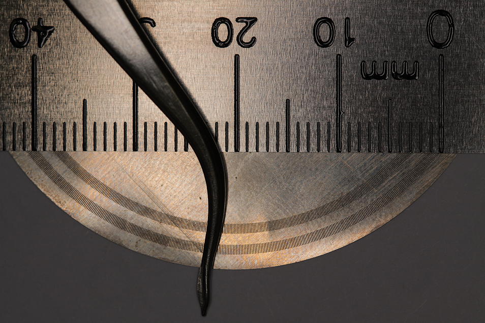
The photo-tool, acting like a highly precise stencil, is the foundation of accuracy. It’s only purpose is coupled with the exposure to UV light. Dimensional tolerances are a function of the thickness of the material. Typically, dimensions can be held to +/- 10 to 15% of the thickness of the material, also better tolerances can be achieved upon request.
Heat sinks and IC Leadframes – (complexity made simple)
Lead-frames and heat sinks – a part commonly used in electrical circuits where heat has to be dissipated. Photo etching can be used in variety of materials such as Phosphorous Bronze and Beryllium copper and/or oxygen free copper. Photo etching is a practical process even in small batches due to the intricacy and fine lines of the part. The components can be fabricated an shipped within 3-5 days, therefore testing can lead into a faster product to market.